
Blackbox for projects that might go up in flames
Links
Idea
During development of a project where data collection is essential, a need for an optically isolated blackbox device arose. This device was designed to be exactly that: it features an optically isolated receive-only UART port and an SD card slot. The firmware receives a binary stream of data, chunks it into SD card pages of 512 bytes, and, using double buffering, writes to the SD card. It has its own lithium battery with a charger to be immune to catastrophic events in other parts of the circuit.
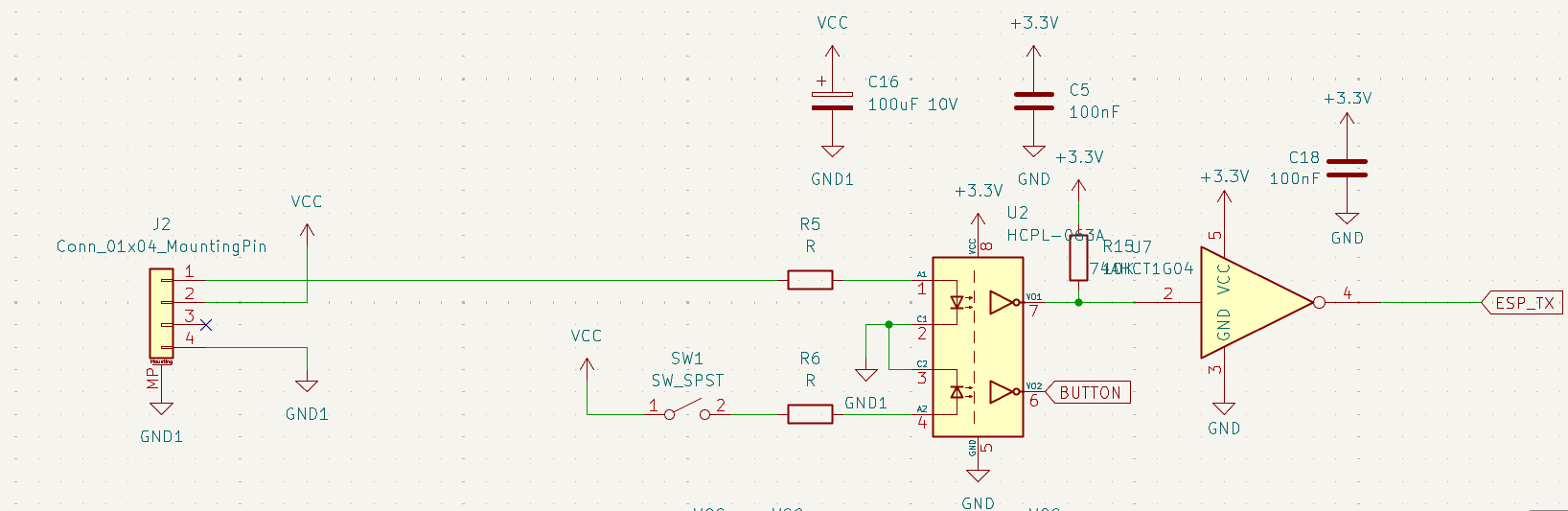
Here is the optical isolation part.
The MCU with SD card, the rest is just power supply and Li-on charger and necessary power and programming connectors.
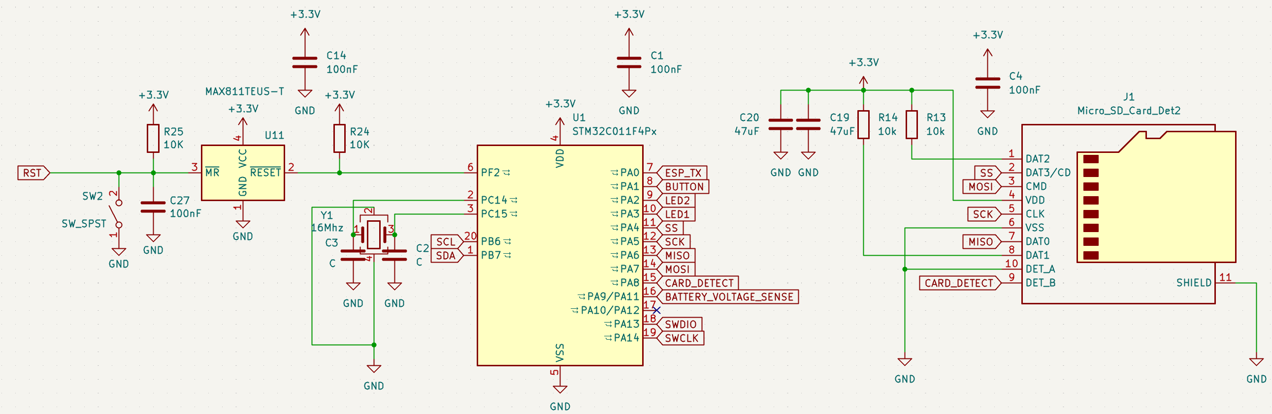
This device utilizes the cheapest STM32 that was in stock on tme.eu at the time of design. It has 16KB of flash and 6KB of RAM. This ended up being not the best idea, as a lot of time was spent during the firmware development on space optimization. In the end, we managed to fit everything with a 4KB DMA buffer (2KB + 2KB in double buffer mode). The baud rate is about 3Mbit/s, which is sufficient for most applications. During testing, we generated orders of magnitude less.
Interface
The PCB features two LEDs and a button. For now, the button is not used, but the LEDs act as a very simple error code display. The first displays error status by either not glowing to state that everything is OK or blinking out the error code value. The next is blinking when the device is properly receiving data from UART.
PCB
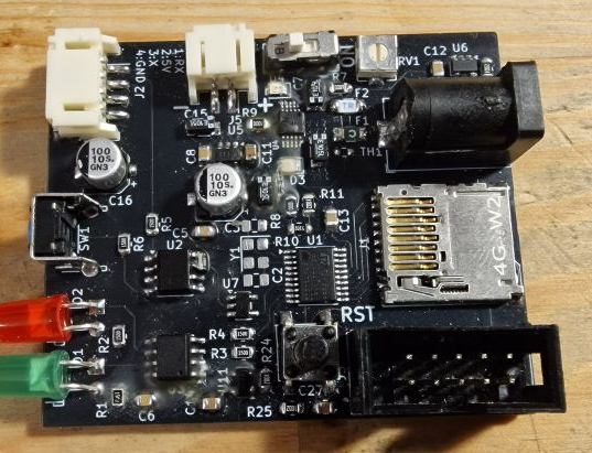
This is how the PCB looks after accounting for all fuckups.
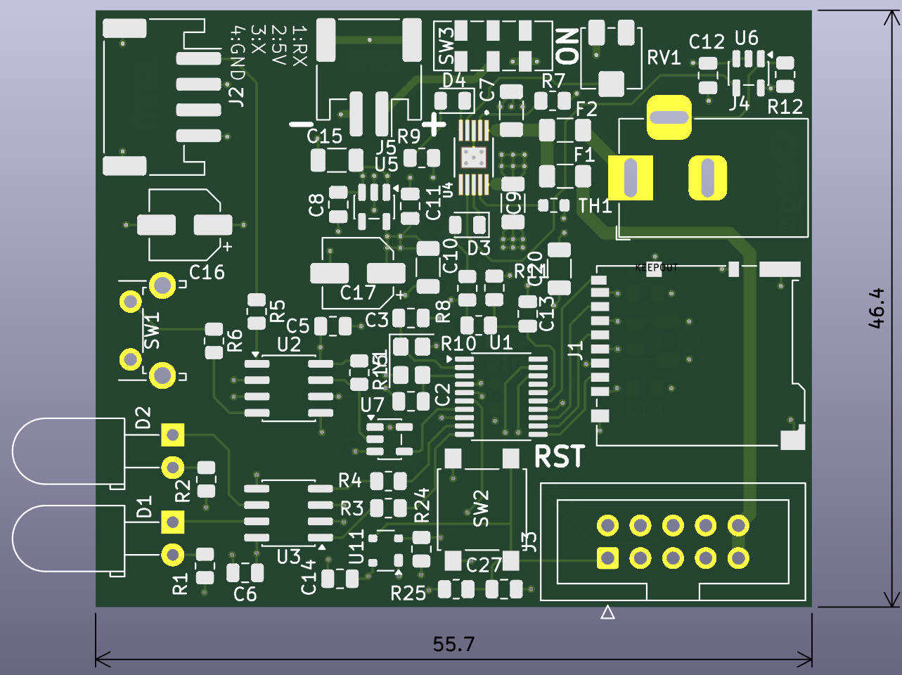
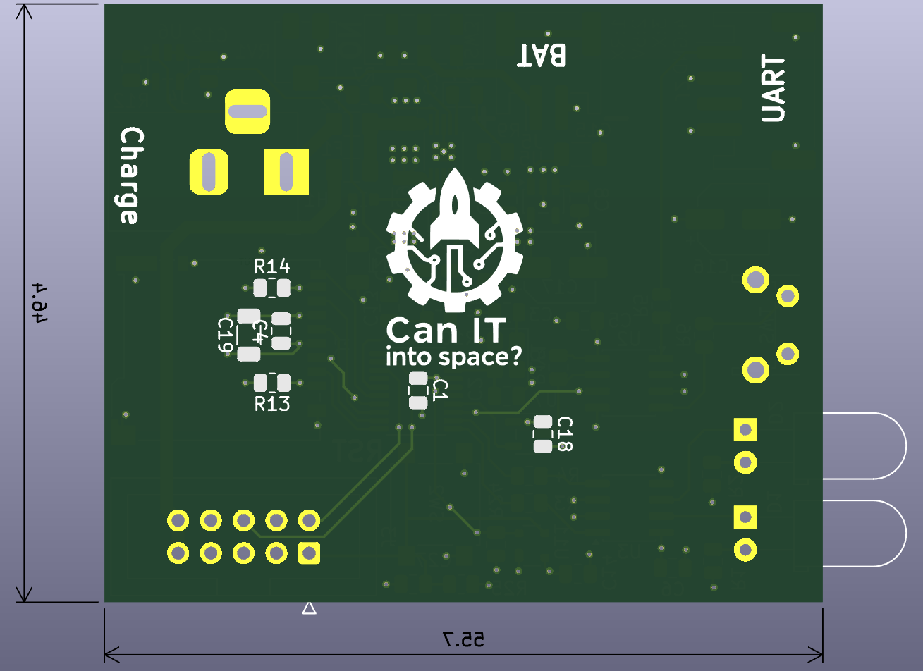
Together with the assembled device. Here you can see the patches applied on PCB, like the SMD resistor soldered directly on the SO8 opto isolator etc… :(
Fuckups (lessons learned)
During the development, several fuckups were made, but the most important ones were:
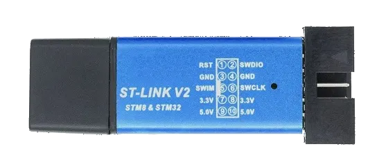
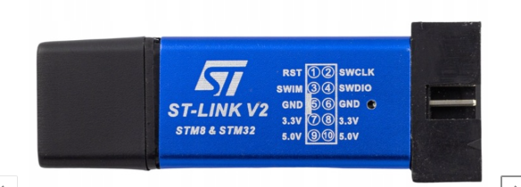
- there are two Chinese ST-Link clone pinouts, and buying them is most of the time a lottery what you will get,
- SD card when hot-swapped into the circuit is VERY power hungry,
- it turned out that SD cards from time to time like to do some housekeeping during which they don’t respond to commands.
Stlink clones
Here are the two pinouts. Unfortunately, the PCB was designed for not the one in my possession. That’s what you get for blindly copying the pinout from Google images.
SD card inrush current
This was way more interesting. During the operation, I tested the hot swapping of the SD card and sometimes encountered a Hard Fault in the STM32. What was very strange was the place in the code of this error. Every time it was somewhere else, and I started suspecting some memory corruption. After some time and a lot of cursing, I commented the entire code out so only basic CPU initialization was left and still got this behaviour. Eventually, I attached my oscilloscope and was stunned to see this upon SD card insertion.
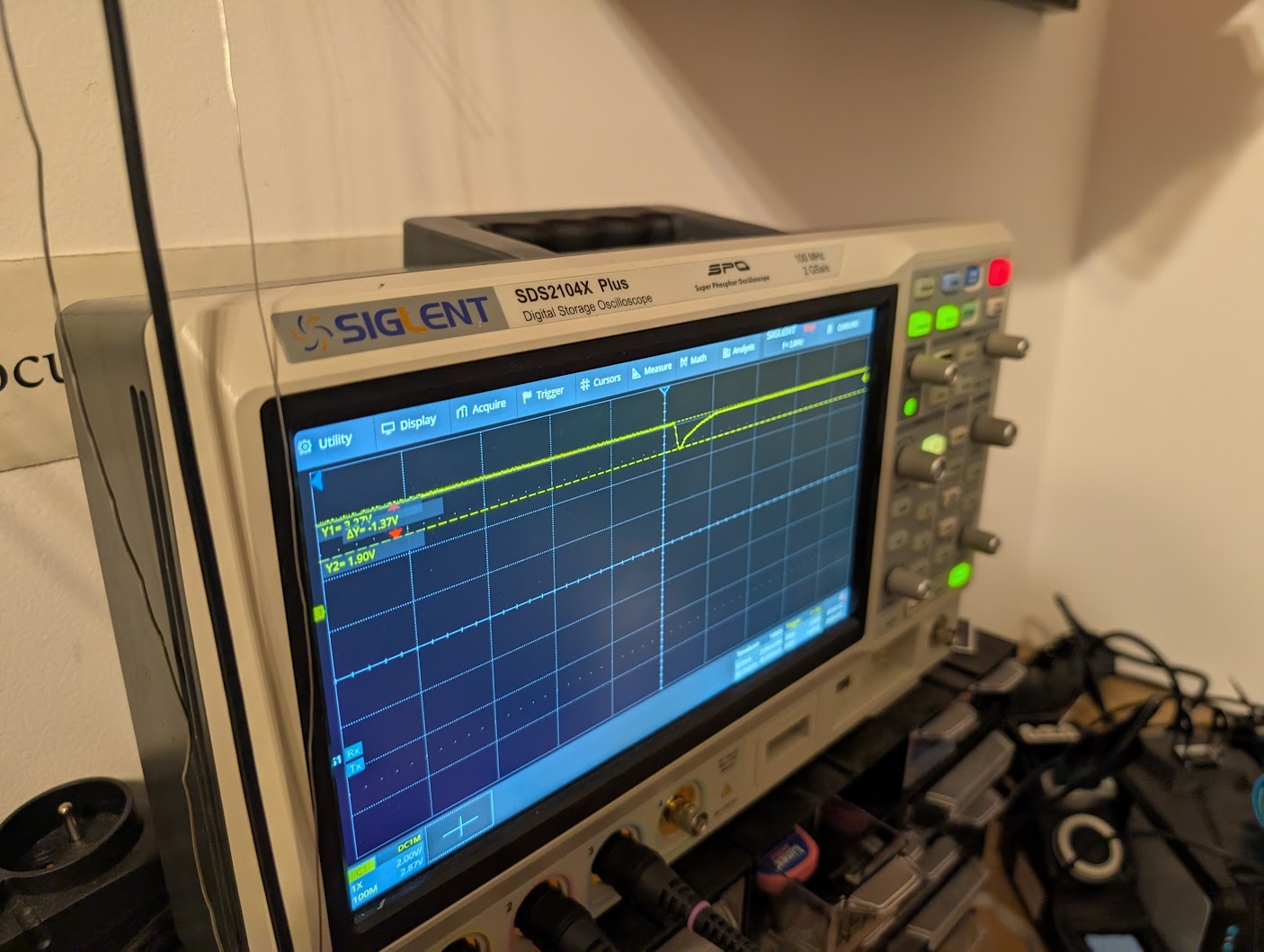
As you can see, the voltage on the main 3.3V power line dips down to 1.9V, which crashes the STM32. This was when I re-educated myself on how to properly design PCBs with SD cards. Basically, the easiest solution is to add WAY MORE CAPACITY IN MMLC; in this case, 30uF got this device to work. A more elegant solution features some buffers and RLC filter to reduce the impact of the inrush current on the rest of the circuit.
Non-industry SD cards are garbage when it comes to latency
To reliably write a data stream to SD cards, you need buffering. It was obvious, just the size of the buffer was a surprise. Apparently, consumer-level SD cards can be sometimes unresponsive for up to 200ms between writes. This is of course necessary for the flash controller to prepare the next flash segment to be written. Unfortunately, it also means that to transfer several Mbits/s of data, you need very large buffers of several 100KB. For my purposes, this STM32 is sufficient, but for higher data rates, a second revision of this board will be created with another MCU.